CXL memory expansion has long been viewed as a way to extend system memory capacity. However, recent advancements are pushing CXL far beyond simple expansion toward fundamentally new memory architectures.
The first implementations of memory expansion typically have modules attached to a host CPU’s CXL bus to augment the local DRAM on the host CPU’s DDR bus. Beyond these first implementations, with the advent of CXL 3.0, memory pooling is being pursued, enabling multiple CPUs to access a common pool of memory through a Multi-Headed Device (MHD) CXL controller. A new use case for CXL technology is to enable very large pools of memory (100s TB – 1 PB), designated as JBOM (Just a Bunch of Memory). JBOM is being pursued to increase the performance of AI Databases and Inference platforms.
While these are exciting developments, from a CXL Controller perspective, it is challenging to plan a chip solution that can meet the diverse requirements of these use cases. In this article, we will show that a chiplet-based architecture is an effective solution for these emerging CXL use cases.
The advantage of chiplet-based architecture is that chiplet building blocks can be assembled at the package level to dial in the desired MHD port number and memory capacity. An example of a chiplet building block implementation is shown in Figure 1, consisting of a CXL port, 2 DDR memory channels (4 DIMMs total), and a Die-to-Die (D2D) connection on each side of the chiplet. The chiplets are then assembled into a package, with NOCs on each chip and D2D connections that allow a CXL port on any chiplet to access the memory attached to any other chiplet. Thus, one can increase the number of chiplets in the package to expand the MHD size for memory pooling or increase the number of chiplets to boost memory capacity via a single CXL port for JBOM.
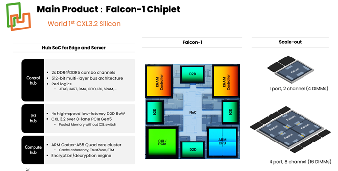
Figure 1: Chiplet building block implementation example with a CXL port, 2 DDR memory channels (4 DIMMs total), and a D2D connection on each side of the chiplet.
Memory Pooling: Enables multiple hosts to access a shared pool of CXL-attached DRAM, dynamically allocating memory across CPUs to enhance workload performance while reducing infrastructure TCO (Total Cost of Ownership). These solutions target 1 TB to 10s of TB, minimize latency and utilize a 1U rack-mount chassis form factor.
One challenge for memory pooling is the availability of cost-effective Multi-Headed Device (MHD) CXL controllers. Ideally, one could connect many Hosts to a CXL controller chip. But designing a monolithic MHD CXL controller chip which can scale beyond 8 ports may require CXL switches. This will be discussed in the next section.
Figure 2 shows an example of how the chiplet approach bypasses these issues, providing a switchless, low-latency 8-port MHD solution.
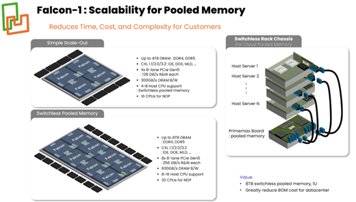
Figure 2: A Chiplet approach providing Switchless, low-latency 8-port MHD solutions
JBOM (Just a Bunch of Memory): For very large pools of memory – 100s of TB to a PB – with 8 or more hosts, CXL switches from third party vendors are required. As shown in Figure 3, Falcon-1 in AIC mode with attached DRAM is connected to CXL switches to form the JBOM pool in a 4U chassis. In this use case, the CXL switch provides better latency than alternatives that use RDMA or require SSD access. The two biggest beneficiaries of JBOM are AI Databases and Inference platforms.
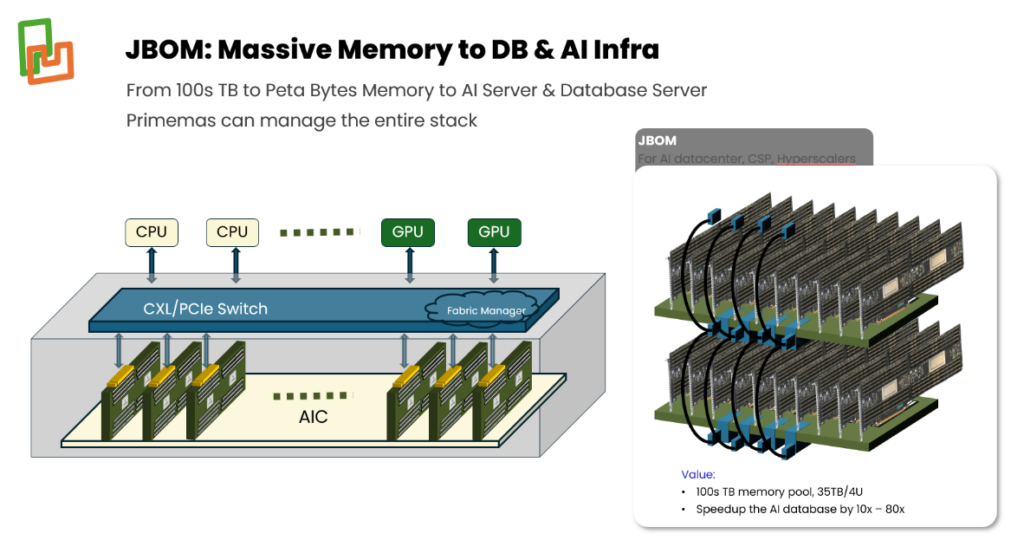
Figure 3: Large pools of CXL memory modules connected through CXL switches
Amongst many use cases for memory pooling, this article discusses (I) AI Databases and (II) KVCache use cases.
(I) AI Database Use Case: Figure 4 shows examples of AI Databases that require large amounts of memory to avoid the added latency from accessing SSD storage. One approach to avoid SSD latency is to use multiple servers to achieve the collective density of the CPU-attached memory and connect the memory between servers through RDMA. This is a costly approach as it requires scaling multiple servers to achieve the desired memory capacity.
However, with a JBOM, memory capacity is achieved with additional CXL memory modules, not by expanding CPUs and their local memory.
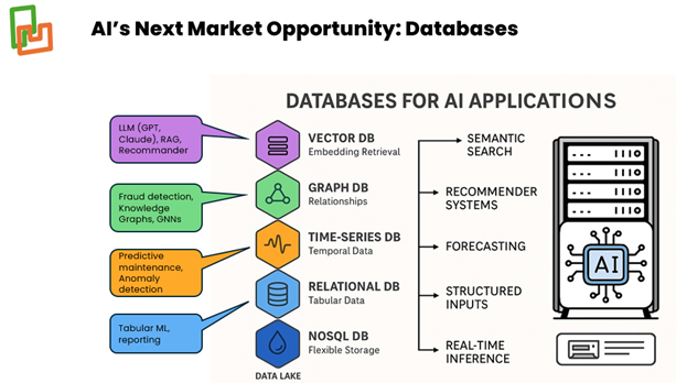
Figure 4: AI Databases require large amounts of memory
(II) For Inference platforms, large data models require large KV Cache memory to achieve high Inference performance, with Time-To-First-Token (TTFT) as a key metric. Because of the limited memory capacity of GPU memory such as HBM (High Bandwidth Memory), systems rely on CPU-attached DRAM memory and pools of memory through RDMA or alternative interconnect schemes to achieve large KV Cache sizes.
However, there is an alternative approach that uses pools of memory accessible by GPUs and CPUs via CXL switches attached to CXL memory modules. This approach was spearheaded by an influential paper by Alibaba Beluga: A CXL-Based Memory Architecture.
In both the AI database and KV Cache, the CXL memory module capacity is very valuable as it enables the highest memory capacity per CXL switch port. In Figure 5, we provide an example of 16 DIMMs per CXL controller package, delivering 2-4 TB per CXL switch port using 128GB-256GB DDR5 DIMMs, respectively.
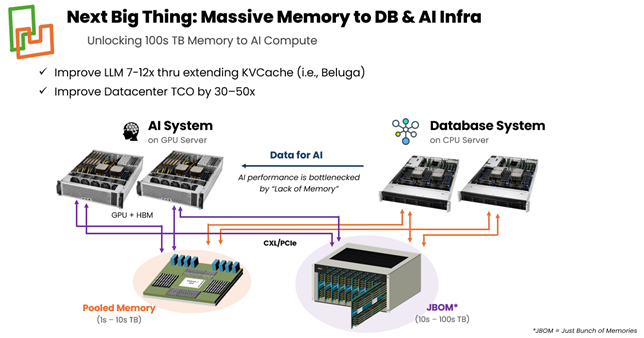
Figure 5: CXL memory module capacity example with 16 DIMMs per CXL controller package, delivering 2-4 TB per CXL switch port using 128GB-256GB DDR5 DIMMs.
Conclusion
New memory architectures, largely driven by AI, are being developed with increasingly diverse requirements. This makes it challenging to develop a portfolio of monolithic CXL controller chip solutions that cover the full range of CXL port counts and memory capacity per port. A chiplet-based CXL controller architecture enables an effective approach to this problem. We have demonstrated with the Primemas Falcon-1 implementation that chiplet architectures enable a single silicon chiplet design to dial in the number of CXL ports and memory capacity at the package level. This approach is particularly valuable for memory pooling by enabling switchless many-port solutions, and for emerging JBOM memory pooling technology by maximizing the memory capacity per CXL switch port. Learn more by visiting https://www.primemas.com/.